Product Summary
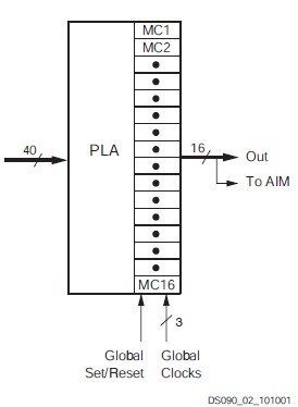
The XC2C64A-7VQG100C is a fast, low power CPLD. The underlying architecture is a traditional CPLD architecture combining macrocells into Function Blocks (FBs) interconnected with a global routing matrix, the Xilinx Advanced Interconnect Matrix (AIM). The Function Blocks use a Programmable Logic Array (PLA) configuration which allows all product terms to be routed and shared among any of the macrocells of the FB. Design software can efficiently synthesize and optimize logic that is subsequently fit to the FBs and connected with the ability to utilize a very high percentage of device resources. Design changes are easily and automatically managed by the software, which exploits the 100% routability of the Programmable Logic Array within each FB. This extremely robust building block delivers the industry highest pinout retention, under very broad design conditions. The XC2C64A-7VQG100C will be explained by expanding the detail as we discuss the underlying Function Blocks, logic and interconnect. The design software automatically manages the XC2C64A-7VQG100C so that users can express their designs using completely generic constructs without knowledge of these architectural details. More advanced users can take advantage of these details to more thoroughly understand the software choices and direct its results.
Parametrics
XC2C64A-7VQG100C absolute maximum ratings: (1)VCC Supply voltage relative to GND: –0.5 to 2.0 V; (2)VI Input voltage relative to GND: –0.5 to 4.0 V; (3)TJ Maximum junction temperature: –40 to 150 ℃; (4)TSTR Storage temperature: –65 to 150 ℃.
Features
XC2C64A-7VQG100C features: (1)Optimized for 1.8V systems; (2)Industry fastest low power CPLD; (3)Densities from 32 to 512 macrocells; (4)Industry best 0.18 micron CMOS CPLD; (5)Optimized architecture for effective logic synthesis; (6)Multi-voltage I/O operation ?1.5V to 3.3V; (7)1.8V ISP using IEEE 1532 (JTAG) interface; (8)On-The-Fly Reconfiguration (OTF); (9)IEEE1149.1 JTAG Boundary Scan Test; (10)Optional Schmitt trigger input (per pin); (11)Multiple I/O banks on all devices; (12)Unsurpassed low power management; (13)Abundant product term clocks, output enables and set/resets; (14)Efficient control term clocks, output enables and set/resets for each macrocell and shared across function blocks; (15)Advanced design security; (16)Open-drain output option for Wired-OR and LED drive; (17)Optional bus-hold, 3-state or weak pullup on select I/O pins; (18)Optional configurable grounds on unused I/Os; (19)Mixed I/O voltages compatible with 1.5V, 1.8V, 2.5V, and 3.3V logic levels on all parts; (20)SSTL2_1,SSTL3_1, and HSTL_1 on 128 macrocell and denser devices; (21)Hot pluggable.
Diagrams

| Image | Part No | Mfg | Description |  |
Pricing (USD) |
Quantity | ||||||||||
|---|---|---|---|---|---|---|---|---|---|---|---|---|---|---|---|---|
 |
 XC2C64A-7VQG100C |
 |
 IC CR-II CPLD 64MCELL 100-VQFP |
 Data Sheet |

|
|
||||||||||
| Image | Part No | Mfg | Description |  |
Pricing (USD) |
Quantity | ||||||||||
 |
 XC2C128 |
 Other |
 |
 Data Sheet |
 Negotiable |
|
||||||||||
 |
 XC2C128-6CPG132C |
 |
 IC CR-II CPLD 128MCELL 132CSBGA |
 Data Sheet |

|
|
||||||||||
 |
 XC2C128-6TQG144C |
 |
 IC CR-II CPLD 128MCELL 144-TQFP |
 Data Sheet |

|
|
||||||||||
 |
 XC2C128-6VQG100C |
 |
 IC CR-II CPLD 128MCELL 100-VQFP |
 Data Sheet |

|
|
||||||||||
 |
 XC2C128-7CPG132C |
 |
 IC CR-II CPLD 128MCELL 132-BGA |
 Data Sheet |

|
|
||||||||||
 |
 XC2C128-7CPG132I |
 |
 IC CR-II CPLD 128MCELL 132CSBGA |
 Data Sheet |

|
|
||||||||||
 (China (Mainland))


